
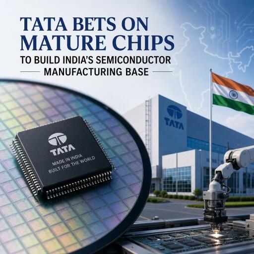

Tata bets on mature chips to build India’s semiconductor manufacturing base
India’s biggest industrial house is stepping onto the silicon stage with a plan that prioritizes resilience over headline-grabbing specs. In collaboration with Taiwan’s Powerchip Semiconductor Manufacturing Corporation (PSMC), Tata is building a foundry blueprint around trusted, higher-yield process nodes—an approach designed to seed a robust domestic ecosystem before attempting the ultra-complex frontier of cutting-edge chips. For the broader tech scene—including gaming and virtual reality—this could quietly reshape supply chains that underpin everything from controllers and sensors to networking and power management.
Why “mature” nodes are a smart opening move
While much of the buzz fixates on 3nm and beyond, a huge slice of modern electronics runs on established nodes. Tata’s new facility at Dholera in Gujarat is expected to span roughly 28nm to 110nm, with initial production targeting 55nm and 90nm. These processes power the electronics that keep industries humming: automotive control units, industrial and medical devices, connectivity modules, smart appliances, and the power chips that regulate and protect them.
For gaming and VR, this is especially relevant. Many of the unsung heroes inside headsets, consoles, and peripherals—wireless controllers, haptics drivers, battery management ICs, sensor hubs, microcontrollers, and connectivity chipsets—are commonly built on these mature nodes. Getting reliable, local capacity for those parts can mean steadier product launches, fewer bottlenecks, and more predictable pricing for manufacturers building in or sourcing from India.
The Dholera blueprint: scale first, then shrink
Jumping straight to the bleeding edge demands extreme ultraviolet (EUV) lithography, elite process engineering teams, and extraordinarily complex supplier networks. That path can drain capital and patience before a single wafer ships. Tata’s phased rollout instead aims for dependable output, training, and process discipline at nodes that are better understood by global suppliers and easier to ramp without painful yield surprises.
By concentrating first on 55nm and 90nm, the project reduces early risk while building a workforce fluent in cleanroom operations, equipment maintenance, and quality control. It also aligns production with markets that have durable, high-volume demand. Once stable manufacturing is in place, shifting down to 40nm, 28nm, and other nodes becomes far more practical—both financially and operationally.
Skipping EUV—for now—strengthens the foundation
EUV tools are some of the most expensive and technically demanding machines on the planet. Avoiding them in the opening act brings multiple benefits: faster time to production, fewer supply-chain choke points, and a smoother learning curve for new talent. In a climate where component shortages can ripple across entire product lines, building capacity for proven nodes tackles an immediate pain point felt by automotive suppliers, appliance makers, industrial integrators, and consumer electronics brands.
For VR and gaming hardware, this translates to shorter lead times for critical support silicon. Even if the most advanced CPUs and GPUs remain the domain of top-tier foundries abroad, steady access to the “everything else” chips can reduce delays for headsets, accessories, and console revisions—especially important in cycles when demand spikes unpredictably.
Policy tailwinds and the path to advanced capability
The initiative dovetails with India’s push to cultivate a full-stack semiconductor value chain. Incentives and policy support are encouraging domestic fabs, packaging, testing, and ancillary suppliers. Rather than trying to outgun established giants from day one, the Tata–PSMC approach focuses on durable industrial capability: reliable yields, local talent pipelines, and a supplier base that can grow in step with the fab’s complexity.
If executed well, the strategy could curb import dependence, draw major electronics manufacturers to set up or expand in India, and create thousands of technical jobs. It also lays the groundwork for future moves into more advanced nodes when timing, talent, and tooling align. That progression—mature today, advanced tomorrow—is how many successful chip ecosystems have scaled without overextending.
What it means for gamers and VR creators
- Greater availability of support silicon: Power management, microcontrollers, RF/connectivity, sensor hubs, and haptics drivers often live on mature nodes. Local capacity reduces vulnerability to global crunches.
- More predictable launches: With fewer component bottlenecks, console refreshes, peripheral rollouts, and headset iterations can hit calendars with greater confidence.
- Potential cost stability: Shipping less silicon across continents and smoothing procurement can help tame price swings in accessory and mid-tier device segments.
- Stronger ecosystem for assembly and testing: As fabs anchor the region, adjacent capabilities in OSAT, modules, and subassemblies typically follow—good news for end-to-end XR manufacturing hubs.
The long game
Building a world-class fab network is a marathon, not a sprint. By prioritizing nodes with proven demand and reliable yields, Tata and PSMC are betting on momentum and mastery before miniaturization. The near-term wins—jobs, supply security, and industrial know-how—feed directly into the harder challenge of pushing toward smaller geometries later.
For the gaming and VR communities, the significance may feel subtle at first. But as component pipelines stabilize and regional manufacturing clusters mature, the impact will be felt in steadier hardware cycles, fewer delays, and a stronger foundation for the next wave of immersive devices. It’s not the flashiest chapter in chipmaking, but it might be the one that ensures the story keeps moving.