
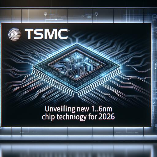

TSMC Unveils Revolutionary 1.6nm Chip Technology Set to Transform Future Devices by 2026
In a significant leap forward in semiconductor technology, TSMC has introduced a new frontier in chip manufacturing with the unveiling of its 1.6nm process technology, labeled as A16. This development, announced during the prestigious North America Technology Symposium, marks a pivotal moment in the semiconductor industry, promising to bring about a new era of faster, more efficient devices ranging from smartphones to complex computing systems.
The advancement to a 1.6nm node process from TSMC, the world’s leading semiconductor manufacturing company, means a substantial increase in transistors on a chip. This boost in transistor density is crucial for enhancing computational performance while simultaneously reducing energy consumption. These improvements are vital for the next generation of electronic devices, ensuring they are not only quicker but also more power-efficient.
Compared to its predecessor, the N2P 2-nanometer process, the new A16 technology by TSMC promises notable enhancements. Specifically, the A16 technology aims to deliver an 8 to 10 percent increase in speed for the same voltage and chip size, alongside a noteworthy 15 to 20 percent decrease in power usage. This improvement is a testament to TSMC’s continual push towards more efficient and robust chip fabrication techniques.
One of the standout features of the A16 process is the introduction of the Super Power Rail (SPR) technology. This innovative approach involves the deployment of power rails to the chip’s rear, enabling an increased density of signal rails on the front. This method, a form of backside power delivery architecture, is a significant step forward in enhancing transistor density and efficiency in power delivery, setting a new benchmark that surpasses earlier initiatives by industry peers.
The potential applications of this groundbreaking technology span various sectors, with particular interest from AI-driven companies. Given Apple’s recent strides into AI and its longstanding partnership with TSMC, it’s anticipated that the new chip technology will be integrated into future Apple-designed chips. This move could spell a considerable uplift in performance and efficiency for upcoming Apple devices.
Historically, Apple devices are among the first to benefit from TSMC’s innovations in chip manufacturing. This trend is expected to continue with the integration of 1.6nm chip technology, potentially starting with the iPhone 18 range slated for 2026. However, while the technology debuts in 2026, its full adoption in commercial products may not occur until the following year, providing a tantalizing glimpse into the future capabilities of smartphones and other electronic devices.
In the interim, Apple is set to utilize TSMC’s 2nm process for its 2026 iPhone models, marking a progressive step from the 3nm technology used in current offerings. The switch signifies ongoing advancements in chip technology, ensuring subsequent iPhone models, such as the iPhone 16 and 17, will see continuous improvements in performance and power efficiency. These advancements are crucial for supporting the evolving demands of modern applications, including enhanced AI capabilities across devices.
The impending A18 chip, expected to feature in the iPhone 16, will embrace the N3E production process, signifying another stride towards better performance and reduced power consumption. Furthermore, this trajectory of using the most advanced chip technology extends beyond the iPhone, with Apple keen on standardizing this across its flagship products, including iPads and Macs. For instance, the introduction of the 3nm-based A17 Pro chip in the iPhone 15 Pro and the subsequent rollout of the M3 chip for the MacBook Pro underscore this strategy.
As TSMC continues to push the boundaries of chip manufacturing technology, the broader industry and consumers alike await with bated breath the wide-ranging implications of the 1.6nm process. This technological marvel holds the promise of redefining what is possible in the realm of electronic devices, setting the stage for a future where computational power and efficiency are in perfect harmony.